- 您现在的位置:买卖IC网 > Sheet目录3875 > PIC18F44J10-I/ML (Microchip Technology)IC PIC MCU FLASH 8KX16 44QFN
PIC16F8X
DS30430C-page 28
1998 Microchip Technology Inc.
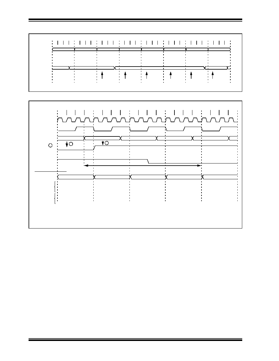
FIGURE 6-3:
TMR0 TIMING: INTERNAL CLOCK/PRESCALE 1:2
FIGURE 6-4:
TMR0 INTERRUPT TIMING
PC-1
Q1 Q2 Q3 Q4 Q1 Q2 Q3 Q4 Q1 Q2 Q3 Q4 Q1 Q2 Q3 Q4 Q1 Q2 Q3 Q4 Q1 Q2 Q3 Q4 Q1 Q2 Q3 Q4 Q1 Q2 Q3 Q4
PC
Instruction
Fetch
TMR0
PC
PC+1
PC+2
PC+3
PC+4
PC+5
PC+6
T0
NT0+1
MOVWF TMR0
MOVF TMR0,W
Write TMR0
executed
Read TMR0
reads NT0
Read TMR0
reads NT0
Read TMR0
reads NT0
Read TMR0
reads NT0
Read TMR0
reads NT0 + 1
T0+1
NT0
Instruction
Execute
Q2
Q1
Q3
Q4
Q2
Q1
Q3
Q4
Q2
Q1
Q3
Q4
Q2
Q1
Q3
Q4
Q2
Q1
Q3
Q4
1
OSC1
CLKOUT(3)
TMR0 timer
T0IF bit
(INTCON<2>)
FEh
GIE bit
(INTCON<7>)
INSTRUCTION FLOW
PC
Instruction
fetched
PC
PC +1
0004h
0005h
Instruction
executed
Inst (PC)
Inst (PC-1)
Inst (PC+1)
Inst (PC)
Inst (0004h)
Inst (0005h)
Inst (0004h)
Dummy cycle
FFh
00h
01h
02h
Note 1: T0IF interrupt flag is sampled here (every Q1).
2: Interrupt latency = 3.25Tcy, where Tcy = instruction cycle time.
3: CLKOUT is available only in RC oscillator mode.
4
Interrupt Latency(2)
4: The timer clock (after the synchronizer circuit) which increments the timer from FFh to 00h immediately sets the T0IF bit.
The TMR0 register will roll over 3 Tosc cycles later.
发布紧急采购,3分钟左右您将得到回复。
相关PDF资料
PIC16F628A-I/P
IC MCU FLASH 2KX14 EEPROM 18DIP
PIC18F24K22-I/SO
IC PIC MCU 16KB FLASH 28SOIC
PIC18F23K22-I/SP
IC PIC MCU 8KB FLASH 28SPDIP
PIC18LF23K22-I/SP
IC PIC MCU 8KB FLASH 28SPDIP
PIC24F08KA102-I/SS
IC PIC MCU FLASH 8K 28-SSOP
PIC16C58B-20/SO
IC MCU OTP 2KX12 18SOIC
PIC12C672-04/SM
IC MCU OTP 2KX14 A/D 8-SOIJ
PIC18F25K20-E/SS
IC PIC MCU FLASH 16KX16 28-SSOP
相关代理商/技术参数
PIC18F44J10-I/P
功能描述:8位微控制器 -MCU 16 KB FL 1024 RAM RoHS:否 制造商:Silicon Labs 核心:8051 处理器系列:C8051F39x 数据总线宽度:8 bit 最大时钟频率:50 MHz 程序存储器大小:16 KB 数据 RAM 大小:1 KB 片上 ADC:Yes 工作电源电压:1.8 V to 3.6 V 工作温度范围:- 40 C to + 105 C 封装 / 箱体:QFN-20 安装风格:SMD/SMT
PIC18F44J10-I/PT
功能描述:8位微控制器 -MCU 16 KB FL 1 KB RAM RoHS:否 制造商:Silicon Labs 核心:8051 处理器系列:C8051F39x 数据总线宽度:8 bit 最大时钟频率:50 MHz 程序存储器大小:16 KB 数据 RAM 大小:1 KB 片上 ADC:Yes 工作电源电压:1.8 V to 3.6 V 工作温度范围:- 40 C to + 105 C 封装 / 箱体:QFN-20 安装风格:SMD/SMT
PIC18F44J10T-I/ML
功能描述:8位微控制器 -MCU 16 KB FL 1024 RAM RoHS:否 制造商:Silicon Labs 核心:8051 处理器系列:C8051F39x 数据总线宽度:8 bit 最大时钟频率:50 MHz 程序存储器大小:16 KB 数据 RAM 大小:1 KB 片上 ADC:Yes 工作电源电压:1.8 V to 3.6 V 工作温度范围:- 40 C to + 105 C 封装 / 箱体:QFN-20 安装风格:SMD/SMT
PIC18F44J10T-I/PT
功能描述:8位微控制器 -MCU 16 KB FL 1024 RAM RoHS:否 制造商:Silicon Labs 核心:8051 处理器系列:C8051F39x 数据总线宽度:8 bit 最大时钟频率:50 MHz 程序存储器大小:16 KB 数据 RAM 大小:1 KB 片上 ADC:Yes 工作电源电压:1.8 V to 3.6 V 工作温度范围:- 40 C to + 105 C 封装 / 箱体:QFN-20 安装风格:SMD/SMT
PIC18F44J11-I/ML
功能描述:8位微控制器 -MCU 16KB Flash 4KBRAM 12MIPS nanoWatt RoHS:否 制造商:Silicon Labs 核心:8051 处理器系列:C8051F39x 数据总线宽度:8 bit 最大时钟频率:50 MHz 程序存储器大小:16 KB 数据 RAM 大小:1 KB 片上 ADC:Yes 工作电源电压:1.8 V to 3.6 V 工作温度范围:- 40 C to + 105 C 封装 / 箱体:QFN-20 安装风格:SMD/SMT
PIC18F44J11-I/PT
功能描述:8位微控制器 -MCU 16KB Flash 4KBRAM 12MIPS nanoWatt RoHS:否 制造商:Silicon Labs 核心:8051 处理器系列:C8051F39x 数据总线宽度:8 bit 最大时钟频率:50 MHz 程序存储器大小:16 KB 数据 RAM 大小:1 KB 片上 ADC:Yes 工作电源电压:1.8 V to 3.6 V 工作温度范围:- 40 C to + 105 C 封装 / 箱体:QFN-20 安装风格:SMD/SMT
PIC18F44J11T-I/ML
功能描述:8位微控制器 -MCU 16KB Flash 4KBRAM 12MIPS nanoWatt RoHS:否 制造商:Silicon Labs 核心:8051 处理器系列:C8051F39x 数据总线宽度:8 bit 最大时钟频率:50 MHz 程序存储器大小:16 KB 数据 RAM 大小:1 KB 片上 ADC:Yes 工作电源电压:1.8 V to 3.6 V 工作温度范围:- 40 C to + 105 C 封装 / 箱体:QFN-20 安装风格:SMD/SMT
PIC18F44J11T-I/PT
功能描述:8位微控制器 -MCU 16KB Flash 4KBRAM 12MIPS nanoWatt RoHS:否 制造商:Silicon Labs 核心:8051 处理器系列:C8051F39x 数据总线宽度:8 bit 最大时钟频率:50 MHz 程序存储器大小:16 KB 数据 RAM 大小:1 KB 片上 ADC:Yes 工作电源电压:1.8 V to 3.6 V 工作温度范围:- 40 C to + 105 C 封装 / 箱体:QFN-20 安装风格:SMD/SMT